
The past few years have been stellar for Artificial Intelligence, thanks to the introduction of generative systems such as ChatGPT. But for this trajectory to continue, AI systems will need to become less artificial and more brain-like. Jon Evans reports
Belying their name, today’s Artificial Intelligence (AI) systems are already less artificial than one might imagine. Based on artificial neural networks (ANNs), they comprise arrays of connected nodes designed to mimic networks of neurons within the human brain. The precise output of these AI systems depends on how connections between the nodes are weighted, which can change with experience. In the same way the output of a specific neuron depends on the precise combination of excitatory and inhibitory signals it receives from other neurons.
By altering the weightings between the nodes, the idea is to train the network to associate specific inputs with a specific output until this produces the desired result. Once trained, these ANNs can do everything from recognise someone’s face to produce bespoke text on a topic of your choice. But while these ANNs may be mimicking brain neurons, they are realised within software running on the digital architecture found in computers. This essentially comprises a chip-based central processing unit (CPU) for doing calculations and a memory unit for storing the results, with the two units linked by a communication pathway.
In the brain, by contrast, the same networks of neurons conduct both processing and storage. This makes the brain much more efficient than a computer, as it doesn’t need to shunt data between physically separate processing and memory units and can do many more calculations in parallel. As such, it can operate at exaflop speeds, or a billion billion calculations/second, using just 20W of energy. In contrast, an ANN operating at such speeds would burn through a hefty 8MW (8 x 10⁶ W).
As more and larger AI systems are trained and used, this level of energy use is raising concerns. The International Energy Agency, for example, predicts that electricity demand from the data centres that house AI systems will grow strongly to at least 2030. There is thus a big question over whether existing electricity systems can meet this rapidly growing demand, which will happen at the same time as most countries are trying to reduce their emissions from power generation. One way to square this circle is to implement ANNs on hardware that more closely mimics the neurons in the brain and thereby try to get closer to its energy efficiency. Fortunately, there is an electronic component, called a memristor, that could potentially fulfil this role.
A memristor is a type of resistor – its name is a contraction of ‘memory resistor’ – whose conductivity depends on the voltages it has been exposed to, like how the activity of a neuron depends on the signals it receives from other neurons. Furthermore, this conductivity can potentially vary between many different values, rather than being just on or off like a transistor – again like the varying activity of the neurons in the brain. Because a memristor can adopt a range of fixed conductivity values, it can conduct calculations. And because the conductivity level persists over time, even when the power is switched off, it can also store the results of those calculations. Thus, it combines processing and memory, just like the neurons in the brain.
A memristor could still act like a transistor, by simply switching between a high conductivity and low conductivity state and so could be combined into the logic gates that process data in today’s CPUs. But, by moving between multiple conductivity values, memristors could also conduct a different type of data processing. This would allow them to multiply matrices together, which is how the weightings in ANNs are calculated, making them potentially ideal hardware for implementing ANNs.
Although memristors were first proposed in the early 1970s, it wasn’t until 2008 that researchers at Hewlett-Packard Laboratories managed to fabricate one, by sandwiching a thin film of titanium dioxide between metal electrodes. Since then, various versions have been developed from a range of materials, including other metal oxides and phase-change materials. But they all work in the same basic way: by concentrating specific charge carriers into a small area or dispersing them over a large area. This is done by applying positive and negative voltages, with one concentrating the charge carriers and the other dispersing them.
As the conductivity of these materials depends on the size of the area containing the charge carriers, the conductivity can be varied over a wide range of values by simply applying a strong enough positive or negative voltage for a certain time period. And because the areas can only be influenced by applying a strong enough voltage, the precise conductivity value persists when the power is switched off.
Nevertheless, memristors remain an immature technology and the ones developed so far suffer from performance issues. They also initially struggled to find a niche. With transistors continually shrinking and CPUs thus getting ever faster, there was no great impetus to investigate the different approaches to computing offered by memristors. The rise of AI has changed all that, and there is now growing interest in seeing whether memristors can help to usher in a more energy efficient, brain-like form of computing, termed neuromorphic computing. This interest is also spurring researchers to explore a variety of other approaches for fabricating memristors, in the hope of developing versions with improved properties and performance that can form the basis for ANNs.
Several researchers are looking to produce memristors from 2D materials like graphene and the transition metal dichalcogenides (TMDs), which consist of a single layer of atoms or molecules. A team led by Harish Bhaskaran at the University of Oxford, UK, recently explored this option by vertically stacking layers of molybdenum disulfide (MoS2) and tungsten disulfide (WS2), both of which are TMDs, with a layer of graphene on a silicon wafer, forming a heterojunction (Nature Nanotech., 2023, 18, 1036).
Bhaskaran and his team showed that not only could the conductivity of this heterojunction be altered by applying a voltage, making it a memristor, but it could also be altered by shining light on it, making it a completely novel type of memristor. This means that the conductivity of the heterojunction can be finely tuned by exposing it to a sequence of voltage and light pulses, just like the activity of a neuron is controlled by the sequence of excitatory and inhibitory signals it receives from other neurons.
Once again, this novel memristor works by confining charge carriers, but in specific layers of the heterojunction. ‘When you shine a light on the device and you apply a certain negative voltage, what happens is a lot of charges get transferred into the graphene,’ explains Bhaskaran. ‘Because you’re monitoring the current through this graphene and there are a lot of charges already in there, you inhibit the movement of the charges and therefore you create a high resistance [low conductivity] state. In the other state, shining the light moves the charges away and the graphene becomes really conductive, and you end up with a low resistance state.’
Meanwhile, a group led by James De Yoreo at the Pacific Northwest National Laboratory (PNNL) in Richland, US, is beginning to explore the potential of combining synthetic 2D materials with natural materials, specifically silk fibroin, one of the two main proteins making up silk. This follows their discovery of a method for getting silk fibroin to form a highly ordered, crystalline layer on the surface of graphene (Science Adv., 2024, 10, eado4142).
‘Silk has already demonstrated significant potential for application in memristors,’ says De Yoreo. ‘However, our epitaxially grown 2D silk possesses unique properties that make it an even more promising candidate for use in memristors.’ Prime among these properties is that it forms a high-quality interface with the graphene layer.
‘High-quality interfaces are crucial for achieving superior electronic and optoelectronic performance,’ explains PNNL team member Chenyang Shi. ‘2D silk effectively addresses the challenges arising from the mismatch between soft silk proteins and hard, planar substrates, offering innovative opportunities for device tuning and optimisation.’
De Yoreo, Shi and their colleagues are now exploring those opportunities. ‘Our research focuses on understanding and optimising the interface between 2D silk films and conductive substrates to enhance their electronic properties,’ Shi says. ‘We’re also investigating how the crystal structure and tunable properties of silk can be leveraged to achieve stable and reproducible resistance switching behaviour.’
Yet other research groups are taking even more inspiration from neurons. A team led by Aleksandra Radenovic at the Ecole Polytechnique Federale de Lausanne (EPFL) in Switzerland has developed a memristor whose conductivity is determined by the flow of ions (Nature Electronics, 2024, 7, 271). This is similar to the way ions rather than electrons carry signals in neurons.
‘Memristors have already been used to build electronic neural networks, but our goal is to build a nanofluidic neural network that takes advantage of changes in ion concentrations, similar to living organisms,’ Radenovic says.
To produce their memristor, they deposit palladium onto a silicon nitride membrane with a 100nm-wide hole in the centre, under conditions that cause the palladium to form nanoscale islands over the surface of the membrane. Then they deposit a layer of graphene on top of the palladium islands, such that it covers the hole.
When they place this memristor in a solution of positively charged potassium ions and apply a positive voltage, the potassium ions migrate through the channels between the palladium islands and congregate at the hole, causing a blister to form in the graphite layer. This blister increases the conductivity of the memristor and persists when the power is switched off. But when a negative voltage is applied, it causes the potassium ions to disperse and the blister to collapse, reducing the conductivity.
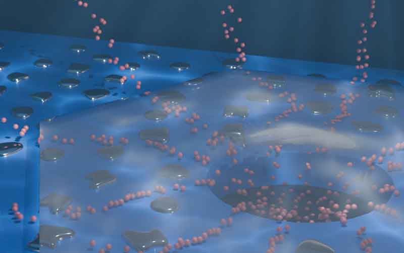
Illustration of potassium ions migrating through the channels between palladium islands to congregate at the hole in a silicon nitride membrane.
Image: ©EPFL 2024 / Andras Kis
Going one step further, a Japanese research team led by Megumi Akai-Kasaya at Osaka University has developed a memristor that looks like a neuron (Adv. Functional Mater., 2023, 33, 2300903). Their memristor is made of a conducting polymer known as PEDOT:PSS and is produced by applying a so-called ‘square-wave’ voltage, which varies over time, to a solution containing precursors to PEDOT:PSS. This causes a network of thin, neuron-like polymer wires to form spontaneously between the electrodes that applied the voltage. Once formed, the conductivity of these polymer wires can be varied by applying small voltage pulses; again, this conductivity persists when the power is switched off.
While still early days, memristors are already beginning to attract commercial interest. ‘We’ve had a few chats with a lot of commercial entities,’ Bhaskaran says. ‘I think they assumed our work is a lot more advanced than it is. So, we had to tell them: “Look, this is research, there needs to be a significant amount of investment to get where it needs to be”.’
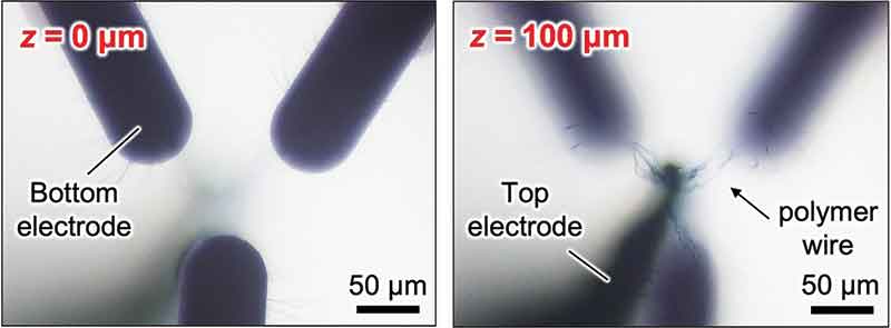
Above: Optical microscopy images of polymer wires forming between a top electrode and three bottom electrodes.
2023 Naruki Hagiwara et al., Advanced Functional Materials.
That investment will be needed not only to turn these fledgling memristors into practical components, but also to address a host of technical challenges. These include how to connect the memristors together into the kind of complex array required for an ANN, and then how to connect them with the conventional computing architecture that will still be required. But this investment will probably come, because the benefits of meeting these challenges are far from artificial.


